Atomic Layer Etching System Market Size to Surpass $2.74 Billion by 2033 | SNS Insider
The U.S. atomic layer etching systems market is estimated at USD 0.36 billion in 2025 and is projected to grow at a CAGR of 8.91% from 2026 to 2033, reaching USD 0.70 billion. Growth is driven by strong semiconductor R&D spending, advanced logic and memory fabrication, adoption of sub-10 nm nodes, demand for precise low-damage etching, and government support for domestic semiconductor manufacturing and reshoring initiatives.
Austin, Jan. 15, 2026 (GLOBE NEWSWIRE) — Atomic Layer Etching System Market Size & Growth Insights:
According to the SNS Insider, “The Atomic Layer Etching System Market size is estimated at USD 1.36 Billion in 2025E and is projected to reach USD 2.74 Billion by 2033, growing at a CAGR of 9.21% during 2026-2033.”
Sub-10nm Scaling GAA Architectures and Advanced Semiconductor Demand is Driving Market Growth Globally
The fast growth of semiconductor devices and the shift to sub-10 nm and gate-all-around (GAA) architectures are the main factors propelling the global market for atomic layer etching (ALE) systems. Conventional etching methods are unable to provide the accuracy, selectivity, and damage control needed in advanced fabrication as device geometries get smaller and structures get more intricate. ALE is crucial for logic, memory, and 3D NAND production because it allows atomic-level material removal with exceptional homogeneity.
Get a Sample Report of Atomic Layer Etching System Market Forecast @ https://www.snsinsider.com/sample-request/9288
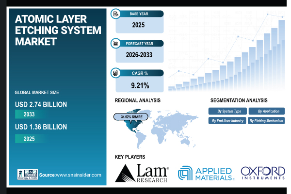
Leading Market Players with their Product Listed in this Report are:
- Lam Research Corporation
- Applied Materials, Inc.
- Tokyo Electron Limited
- Hitachi High-Tech (Hitachi High-Technologies)
- Oxford Instruments
- Samco Inc.
- CORIAL
- Nano Vacuum Pty Ltd
- Plasma-Therm LLC
- NAURA Technology Group
- Mattson Technology, Inc.
- KLA Corporation
- SCREEN Semiconductor Solutions
- Ultratech (KLA)
- MKS Instruments
- SEMES
- ULVAC, Inc.
- SPTS Technologies (KLA)
- AMEC (Advanced Micro-Fabrication Equipment Inc.)
- SENTECH Instruments GmbH
Atomic Layer Etching System Market Report Scope:
| Report Attributes | Details |
| Market Size in 2025 | USD 1.36 Billion |
| Market Size by 2033 | USD 2.74 Billion |
| CAGR | CAGR of 9.21 % From 2026 to 2033 |
| Report Scope & Coverage | Market Size, Segments Analysis, Competitive Landscape, Regional Analysis, DROC & SWOT Analysis, Forecast Outlook |
| Key Segmentation | • By System Type (Thermal Atomic Layer Etching Systems, Plasma Atomic Layer Etching Systems, Radical‐Assisted Atomic Layer Etching Systems, and Cycling Type Atomic Layer Etching Systems) • By Etching Mechanism (Surface Reaction Controlled Etching, Ion‐Assisted Etching, Neutral Radical Etching, and Remote Plasma Etching) • By Application (Semiconductor Device Fabrication, Memory & Logic Devices, MEMS & Sensors Manufacturing, and Compound Semiconductors & Photonics) • By End-User Industry (Semiconductor Foundries, Integrated Device Manufacturers (IDMs), OEMs in Electronics & Communication, and Academic & Research Institutions) |
Purchase Single User PDF of Atomic Layer Etching System Market Report (20% Discount) @ https://www.snsinsider.com/checkout/9288
Process Complexity Limited Standardization and Scalability Challenges May Impede Market Growth Globally
The market for atomic layer etching systems is constrained by the complexity of the process and the lack of uniformity among different types of materials and devices. Adoption is slowed by the need for considerable optimization and advanced process knowledge to integrate ALE into current fabrication procedures. In high-volume manufacturing, limited throughput in comparison to traditional etching might affect productivity. Furthermore, ALE technology is continually developing, facing difficulties with scalability across a range of semiconductor applications, material compatibility, and process repeatability.
Key Segmentation Analysis
By System Type
Plasma Atomic Layer Etching Systems dominated with 43.68% in 2025E due to their wide applicability in logic, memory, and advanced semiconductor fabs, offering precise, high-throughput etching. Radical‐Assisted Atomic Layer Etching Systems is expected to grow at the fastest CAGR of 9.73% from 2026 to 2033 driven by growing demand for ultra-low-damage, high-precision etching in advanced nodes, 3D structures, and new materials, such as GaN, SiC, and high-k dielectrics.
By Etching Mechanism
Ion‐Assisted Etching dominated with 34.65% in 2025E due to its effective directional control, high precision, and compatibility with advanced high-aspect-ratio semiconductor structures. Neutral Radical Etching is expected to grow at the fastest CAGR of 9.94% from 2026 to 2033 driven by rising demand for low-damage, highly selective etching processes in next-generation devices, 3D NAND, MEMS, and compound semiconductor applications.
By Application
Semiconductor Device Fabrication dominated with 39.68% in 2025E driven by widespread adoption of atomic layer etching across logic, memory, and 3D NAND manufacturing for precise, uniform material removal. MEMS & Sensors Manufacturing is expected to grow at the fastest CAGR of 10.43% from 2026 to 2033 fueled by increasing integration of sensors in automotive, IoT, and wearable devices.
By End-User Industry
Semiconductor Foundries dominated with 44.73% in 2025E due to their high-volume production needs and demand for precise, low-defect etching of advanced nodes. OEMs in Electronics & Communication is expected to grow at the fastest CAGR of 10.33% from 2026 to 2033 fueled by rising adoption of miniaturized, high-performance electronic components, expansion in 5G infrastructure, and increasing use of advanced materials requiring precise etching techniques.
Regional Insights:
North America holds a 34.62% share of the Atomic Layer Etching (ALE) system market in 2025, driven by a strong semiconductor manufacturing base in the U.S. and Canada.
Asia Pacific dominates the Atomic Layer Etching (ALE) system market with a 39.49% share in 2025, driven by rapid semiconductor and electronics manufacturing growth in countries like China, South Korea, and Taiwan.
Do you have any specific queries or need any customized research on Atomic Layer Etching System Market? Submit your inquiry here @ https://www.snsinsider.com/enquiry/9288
Recent Developments:
- In September 2025, Lam Research entered into a non‑exclusive cross‑licensing and collaboration agreement with JSR Corporation and its Inpria unit to advance next‑generation semiconductor manufacturing, including work on materials and processes relevant to atomic layer etching and deposition.
- In February 2024, Applied Materials introduced a broad portfolio of angstrom‑era patterning solutions including advanced etch and deposition systems, such as the Sym3® Y Magnum™ etch system, new CVD films, and pattern‑shaping technologies to support leading‑edge nodes at 2 nm and below.
Exclusive Sections of the Atomic Layer Etching System Market Report (The USPs):
- SHARE (%) OF ATOMIC LAYER ETCHING SYSTEMS DEPLOYED AS PLASMA-BASED VERSUS THERMAL-BASED SYSTEMS: Helps you understand technology preference trends across semiconductor fabs and assess capability alignment with precision etching requirements.
- PERCENTAGE (%) OF SEMICONDUCTOR FABS USING ATOMIC LAYER ETCHING FOR ADVANCED NODE MANUFACTURING BELOW 10 NM: Helps you evaluate penetration levels of atomic layer etching in leading-edge semiconductor production and identify adoption maturity.
- AVERAGE NUMBER OF ATOMIC LAYER ETCHING PROCESS STEPS USED PER WAFER IN MEMORY AND LOGIC DEVICE FABRICATION: Helps you assess process complexity, tool utilization intensity, and demand drivers for multi-step etching solutions.
- TECHNOLOGICAL CAPABILITY TO SUPPORT SUB-10 NM AND MULTI-PATTERNING REQUIREMENTS: Helps you identify systems designed for next-generation nodes where precision, selectivity, and uniformity are critical.
- INTEGRATION OF ATOMIC LAYER ETCHING WITH ADVANCED PROCESS CONTROL AND METROLOGY SYSTEMS: Helps you understand the readiness of suppliers to support high-yield manufacturing through tighter process monitoring and control.
About Us:
SNS Insider is one of the leading market research and consulting agencies that dominates the market research industry globally. Our company’s aim is to give clients the knowledge they require in order to function in changing circumstances. In order to give you current, accurate market data, consumer insights, and opinions so that you can make decisions with confidence, we employ a variety of techniques, including surveys, video talks, and focus groups around the world.
CONTACT: Contact Us:
Rohan Jadhav - Principal Consultant
Phone: +1-315 636 4242 (US) | +44- 20 3290 5010 (UK)
 Disclaimer: The above press release comes to you under an arrangement with GlobeNewswire. DailyIndiaNews.com takes no editorial responsibility for the same.