Die-to-Die IP Market Size to Surpass USD 3.72 Billion by 2033 | Research by SNS Insider
The U.S. Die-to-Die IP market was valued at USD 0.51 billion in 2025E and is projected to reach USD 1.02 billion by 2033, growing at a CAGR of 9.17% during 2026–2033. Market growth is driven by strong investments in AI and high-performance computing, rapid adoption of chiplet architectures, leadership in advanced packaging technologies, and rising demand from hyperscalers for high-bandwidth, energy-efficient interconnect solutions.
Austin, Jan. 14, 2026 (GLOBE NEWSWIRE) — Die-to-Die IP Market Size & Growth Insights:
According to the SNS Insider, “The Die-to-Die IP Market Size is estimated at USD 1.80 Billion in 2025 and is projected to reach USD 3.72 Billion by 2033, growing at a CAGR of 9.57% during 2026-2033.”
Rapid Shift to Chiplet Architectures is Boosting Market Growth Globally
The swift shift from monolithic system-on-chip designs to chiplet-based architectures, which allow for increased performance, enhanced yield, and reduced development costs, is the main factor propelling the global Die-to-Die IP market. Ultra-high bandwidth, low latency, and energy-efficient interconnect solutions between numerous dies are needed to meet the growing demand for high-performance computing, AI, machine learning, and data center processors. Interoperability and ecosystem maturity are being accelerated by developments in advanced packaging technologies, such as 2.5D and 3D IC integration as well as the expanding use of open standards, including UCIe.
Get a Sample Report of Die-to-Die IP Market Forecast @ https://www.snsinsider.com/sample-request/9282
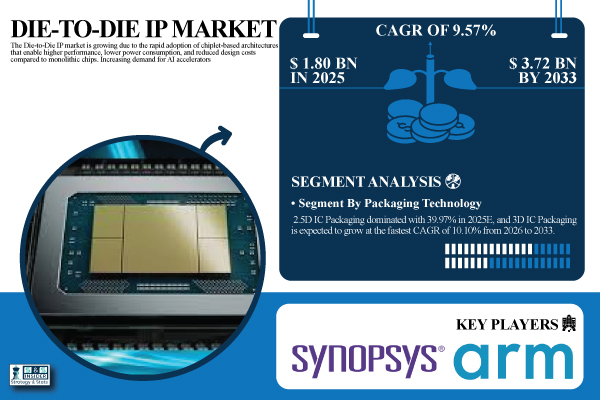 Leading Market Players with their Product Listed in this Report are:
- Synopsys
- Cadence Design Systems
- Arm Holdings
- Marvell Technology
- Alphawave Semi
- Rambus
- Arteris
- Blue Cheetah Analog Design
- VeriSilicon
- OpenFive
- OPENEDGES Technology
- Siemens EDA
- Texas Instruments
- NXP Semiconductors
- Infineon Technologies
- STMicroelectronics
- Renesas Electronics
- Microchip Technology
- Analog Devices
- ON Semiconductor
Die-to-Die IP Market Report Scope:
| Report Attributes | Details |
| Market Size in 2025 | USD 1.80 Billion |
| Market Size by 2033 | USD 3.72 Billion |
| CAGR | CAGR of 9.57 % From 2026 to 2033 |
| Report Scope & Coverage | Market Size, Segments Analysis, Competitive Landscape, Regional Analysis, DROC & SWOT Analysis, Forecast Outlook |
| Key Segmentation | • By Interface Standard (UCIe (Universal Chiplet Interconnect Express), BoW (Bunch of Wires), Proprietary / Custom Interfaces, and Emerging Open Standards) • By Packaging Technology (2.5D IC Packaging, 3D IC Packaging, Fan-Out Wafer-Level Packaging (FOWLP), and System-in-Package (SiP)) • By Application (High-Performance Computing (HPC) & AI Accelerators, Data Centers & Cloud Infrastructure, Consumer Electronics, and Automotive Electronics) • By End-User (Semiconductor Foundries & OSATs, Integrated Device Manufacturers (IDMs), Fabless Semiconductor Companies, and System OEMs & Hyperscalers) |
Purchase Single User PDF of Die-to-Die IP Market Report (20% Discount) @ https://www.snsinsider.com/checkout/9282
Standardization Challenges Complex Designs and Thermal Management Limitations May Impede Market Expansion Globally
Beyond early UCIe adoption, the Die-to-Die IP industry is constrained by a lack of standardization, which makes it difficult for manufacturers and ecosystems to work together. Faster adoption is hampered by advanced packaging’s thermal management limitations, signal integrity problems at high data speeds, and design complexity. Large-scale implementation is also slowed by protracted qualification cycles in industrial and automotive applications, as well as difficulties with IP integration and validation across diverse dies.
Key Segmentation Analysis
By Interface Standard
UCIe (Universal Chiplet Interconnect Express) dominated with 53.43% in 2025 and it is expected to grow at the fastest CAGR of 9.92% from 2026 to 2033 due to its open, interoperable architecture, enabling seamless communication between chiplets from different vendors.
By Packaging Technology
2.5D IC Packaging dominated with 39.97% in 2025E due to its open, interoperable architecture, enabling seamless communication between chiplets from different vendors. 3D IC Packaging is expected to grow at the fastest CAGR of 10.10% from 2026 to 2033 driven by increasing demand for higher interconnect density, improved power efficiency, and advanced heterogeneous integration in AI accelerators, automotive electronics, and next-generation computing systems.
By Application
High-Performance Computing (HPC) & AI Accelerators dominated with 41.86% in 2025 and it is expected to grow at the fastest CAGR of 9.83% from 2026 to 2033 due to the surge in AI workloads, deep learning, and complex simulations requiring ultra-high bandwidth and low-latency interconnects.
By End-User
Semiconductor Foundries & OSATs dominated with 34.99% in 2025E driven by their role in advanced packaging, multi-die integration, and providing scalable solutions for multiple clients across HPC, AI, and automotive applications. Fabless Semiconductor Companies is expected to grow at the fastest CAGR of 10.12% from 2026 to 2033 as they increasingly adopt standardized chiplet architectures and die-to-die IP to accelerate time-to-market, enhance performance, and reduce design complexity, supported by growing collaboration with foundries, system OEMs, and hyperscalers globally.
Regional Insights:
North America, holding 36.36% of the Die-to-Die IP market in 2025E, is the dominant region due to its strong semiconductor ecosystem, presence of leading chiplet and IP vendors, and early adoption of advanced packaging and UCIe standards.
Asia Pacific is expected to register the fastest CAGR of 10.25% from 2026–2033 in the Die-to-Die IP market, driven by rapid semiconductor manufacturing expansion in China, Taiwan, South Korea, and Japan.
Do you have any specific queries or need any customized research on Die-to-Die IP Market? Submit your inquiry here @ https://www.snsinsider.com/enquiry/9282
Recent Developments:
- In September 2024, Synopsys announced a 40 Gbps‑per‑pin UCIe IP suite, including controller, PHY, and verification IP to enable ultra‑high‑bandwidth die‑to‑die connectivity for multi‑die AI data center chips. The solution offers enhanced signal integrity monitoring and broad interconnect support.
- In April 2025, Cadence announced a significant enhancement of its design IP portfolio, including UCIe 1.1 48G die‑to‑die interconnect IP and advanced interface IP optimized for Intel’s 18A and 18A‑P technologies to accelerate AI, HPC, and mobility designs.
Exclusive Sections of the Die-to-Die IP Market Report (The USPs):
- TECHNOLOGICAL ADOPTION RATE – helps you track the penetration of UCIe, BoW, proprietary, and emerging open die-to-die interface standards, along with adoption of high-bandwidth, low-latency, and energy-efficient interconnects.
- PACKAGING & INTERFACE PERFORMANCE METRICS – helps you understand deployment shares across 2.5D, 3D IC, FOWLP, and system-in-package technologies supporting chiplet-based architectures.
- APPLICATION DEMAND & UTILIZATION TRENDS – helps you identify demand concentration across HPC, AI accelerators, hyperscale data centers, consumer electronics, and automotive electronics, including growth rates in high-performance applications.
- CAPACITY UTILIZATION & COMMERCIALIZATION METRICS – helps you assess the share of advanced semiconductor products adopting die-to-die IP, integration cycle times, and commercialization readiness of chiplet designs.
- PRICING & REVENUE PERFORMANCE INDICATORS – helps you evaluate licensing cost variations by interface standard and packaging technology, along with overall market revenue growth trends.
- COMPETITIVE LANDSCAPE & ECOSYSTEM STRENGTH – helps you gauge the market position of leading die-to-die IP providers through licensing-based market share, customer retention rates, and adoption by foundries, IDMs, and fabless companies.
About Us:
SNS Insider is one of the leading market research and consulting agencies that dominates the market research industry globally. Our company’s aim is to give clients the knowledge they require in order to function in changing circumstances. In order to give you current, accurate market data, consumer insights, and opinions so that you can make decisions with confidence, we employ a variety of techniques, including surveys, video talks, and focus groups around the world.
CONTACT: Contact Us:
Rohan Jadhav - Principal Consultant
Phone: +1-315 636 4242 (US) | +44- 20 3290 5010 (UK)
 Disclaimer: The above press release comes to you under an arrangement with GlobeNewswire. DailyIndiaNews.com takes no editorial responsibility for the same.